
For Outstation Students, we are having online project classes both technical and coding using net-meeting software
For details, Call: 9886692401/9845166723
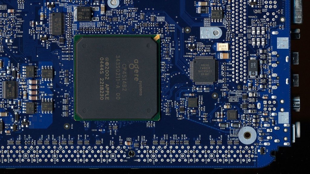
DHS Informatics providing latest 2021 – 2022 IEEE projects on CMOS / VLSI projects for the final year engineering students. DHS Informatics trains all students in VLSI techniques to develop their project with good idea what they need to submit in college to get good marks. DHS Informatics offers placement training in VLSI at Bangalore and the program name is OJT – On Job Training, job seekers as well as final year college students can join in this placement training program and job opportunities in their dream IT companies. We are providing IEEE projects for B.E / B.TECH, M.TECH, MCA, BCA, DIPLOMA students from more than two decades.
Python Final year CSE projects in Bangalore
Abstract:
This brief presents efficient unified hardware for up-to-date authenticated encryptions with associated data (AEADs). Although some major AEADs share several fundamental components (e.g., advanced encryption standard (AES), block chaining, and XOR-Encryption-XOR (XEX) scheme), each AEAD is equipped with a unique mode of operation and/or subfunctions, which makes it difficult to integrate various AEADs in hardware efficiently. The proposed hardware in this brief efficiently unifies the fundamental components to perform a set of AEADs with minimal area and power overheads. The proposed configurable datapath is adapted to a set of peripheral operations (e.g., block chaining and XEX), dictated by the given AEAD algorithm. In this brief, we also demonstrate the validity of the proposed hardware through an experimental design adapted to four AES-based AEADs. Consequently, we confirm that the proposed hardware can perform the four AEADs with a quite smaller area than the sum of each dedicated AEAD hardware, comparable throughput, and power consumption. In addition, we confirmed that the proposed hardware is superior to software implementation on the general-purpose processors in terms of both throughput and power consumption.
Abstract:
Abstract:
Cryptography is the science that concerns protecting data by transforming its comprehensible form into an incomprehensible one. This study aims to compare Advanced Encryption Standard (AES) and Rivest-Shamir-Adleman (RSA) encryption algorithms in image encryption using MATLAB. The comparison is done in the terms of testing image encryption quality for each algorithm. In addition, analyzing the histogram and correlation results. The results showed that the AES algorithm has a better image encryption quality with a more convergent column in the histogram. Moreover, the AES algorithm correlation coefficient tends to be closer to zero, thus a stronger correlation. Generally, the outcomes of this study showed that the AES algorithm is better than the RSA algorithm in image encryption.
Abstract:
Abstract:
Abstract:
As the technology is getting advanced continuously the problem for the security of data is also increasing. The hackers are equipped with new advanced tools and techniques to break any security system. Therefore people are getting more concerned about data security. Data security is achieved by either software or hardware implementations. In this work Field, Programmable Gate Arrays (FPGA) device is used for hardware implementation since these devices are less complex, more flexible, and provide more efficiency. This work focuses on the hardware execution of one of the security algorithms that is the Advanced Encryption Standard (AES) algorithm. The AES algorithm is executed on Vivado 2014.2 ISE Design Suite and the results are observed on 28 nanometers (nm) Artix-7 FPGA. This work discusses the design implementation of the AES algorithm and the resources consumed in implementing the AES design on Artix-7 FPGA. The resources which are consumed are as follows- Slice Register (SR), Look-Up Tables (LUTs), Input/Output (I/O), and Global Buffer (BUFG).
Abstract:
Huffman coding is very important technique in information theory. It is the process of encoding data using fewer bits than an uncompressed data. Furthermore, Clock gating and frequency scaling are efficient techniques for reducing power consumption in sequential design. It saves more power by partitioning the main clock and distributing the clock to the logic blocks only when there is a need for those blocks to be activated. This paper aims to design and implementation of Huffman coding based on binary tree using FPGA (Field Programmable Gate Arrays), and proposing a novel method of clock gating and frequency scaling to achieve low power consumption and reliability of design. The proposed Huffman was achieved 47.95% saving percentage in data size. While, reduce power consumption up to 52.52% comparing to traditional design. Huffman design was implemented by using ASIC and FPGA design methodologies. In order to implement the encoder and decoder architectures, 130 nm standard cell technology libraries were used for ASIC implementation. The simulations are carried out by using Modelsim tool. The architecture of coding and decoding process has been created using Verilog HDL language. Quartus II 11.1 Web Edition (32-Bit). In addition, simulated using ModelSim-Altera 10.0c (Quartus II 11.1) Starter Edition.
.
IEEE The performance of text file compression using Shannon-Fano and Huffman on small mobile devices
Abstract:
Textual information has grown tremendously generated from mobile user to digital libraries and archival text data from many internet sources. Many programs for data compression have been developed. However, mostly are only efficient to read small/brief files but inefficient, not even applicable, for very large files, especially on mobile devices. This is because the algorithm is too heavy to process and the design specification is to read short files that are repeated. In addition, large file sizes when transferred will require longer transfer times, larger space and higher costs, as file transfer rates are affected by internet network speed and file size. Text compression can be considered as a possible best approach in reducing storage space efficiently and accelerate transmission speed. In this study Shanno-Fano and Huffman algorithm has been evaluated and also the possible compression method on smartcard has been discussed. The aim of this study is to produce a compression method that produces text files with the smallest ratios and the fastest compression and de-compression times especially on mobile devices. This study improves file compression performance in order to obtain better file size, compression ratio, and compression time especially on text processing
Abstract:
Data compression in cache memory allows increasing the effective capacity, which improves the hit rate and only insignificantly affects power consumption and die area. In this paper, the results of the first research on cache compression in processors with Elbrus architecture are presented. Base+Delta (B+Δ) and Base-Delta Immediate (BΔI) compression algorithms are selected for hardware implementation for their high efficiency and lower decompression latency compared to other algorithms. The modified versions of these algorithms, B+Δ* and BΔI*, which allow to reduce implementation complexity and further shorten the latency, are presented. Additionally, a new set of compression schemes for modified algorithms (labeled as BΔI*-HL algorithm) is proposed to account for width of the interfaces and internal data buses. The algorithms were implemented using Verilog HDL and evaluated on FPGA prototype of Elbrus-8C2 processor and SPEC CPU2000 benchmark suite. The results show that BΔI* demonstrates almost equal of greater compression ration as the original BÄI algorithm while has significantly lower implementation complexity
Abstract:
This paper provides the study of various lossless data compression techniques and compares their performance and efficiency using time and space complexity. Data compression is itself a huge field in a computer science and it is used in reducing the size of data by removing the redundant characters or encoding the bits in data. We have used only lossless data compression techniques for compressing various media format files like text, doc, bmp, png and wav. Huffman coding which generates variable length codes for each symbol. LZW is a dictionary based technique and Shannon-Fano coding is used to generate binary code based on the frequency of each symbol. So we calculated the mean compression ratio, compression factor and compression time for various media files and result analysis of above data compression techniques will help to select the most appropriate method of compressing of any given file format in real world.
Abstract: Nowadays, the volume of information that is being processed is increasing exponentially. And hence, the significance of data compression algorithms is also increasing. Data compression algorithms aim at reducing the size of data at the cost of increased computational efforts. In this paper, we propose an enhanced version of adaptive Huffman encoding technique for improving the efficiency of text file compression. In the proposed encoding technique, we devise a mechanism for compressing the text files word by word rather than the existing byte by byte compression technique. The proposed method is implemented and the results showed better performance in terms of compression ratio as well as execution time.
IEEE CMOS & VLSI PROJECTS (2021 – 2022)
| S.NO | VLSI BASED PROJECTS | SYNOPSIS |
|---|---|---|
|
1
|
VLSI-FPGA IMPLEMENTATION OF AES ALGORITHM
|
 |
|
2
|
VLSI-FPGA IMPLEMENTATION OF PIPELINED FAST FOURIER TRANSFORM (FFT) ALGORITHM
|
|
|
3
|
VLSI -FPGA IMPLEMENTATION OF GMSK TRANSMITTER
|
|
|
4
|
VLSI-FPGA IMPLEMENTATION OF OFDM IP
|
|
|
5
|
VLSI-FPGA IMPLEMENTATION OF A SINGLE-CYCLE PROCESSOR FOR A SUBSET OF THE MIPS ARCHITECTURE IN VERILOG HDL (HARDWARE DESCRIPTION LANGUAGE)
|
|
|
6
|
VLSI-FPGA IMPLEMENTATION VITERBI DECODER
|
|
DHS Informatics believes in students’ stratification, we first brief the students about the technologies and type of CMOS / VLSI projects and other domain projects. After complete concept explanation of the IEEE CMOS / VLSI projects, students are allowed to choose more than one IEEE CMOS / VLSI projects for functionality details. Even students can pick one project topic from CMOS / VLSI and another two from other domains like CMOS / VLSI, image process, information forensic, big data, and CMOS / VLSI, block chain etc. DHS Informatics is a pioneer institute in Bangalore / Bengaluru; we are supporting project works for other institute all over India. We are the leading final year project centre in Bangalore / Bengaluru and having office in five different main locations Jayanagar, Yelahanka, Vijayanagar, RT Nagar & Indiranagar.
We allow the ECE, CSE, ISE final year students to use the lab and assist them in project development work; even we encourage students to get their own idea to develop their final year projects for their college submission.
DHS Informatics first train students on project related topics then students are entering into practical sessions. We have well equipped lab set-up, experienced faculties those who are working in our client projects and friendly student coordinator to assist the students in their college project works.
We appreciated by students for our Latest IEEE projects & concepts on final year CMOS / VLSI projects for ECE, CSE, and ISE departments.
Latest IEEE 2020 – 2021 projects on CMOS / VLSI with real time concepts which are implemented using Java, MATLAB, and NS2 with innovative ideas. Final year students of computer CMOS / VLSI, computer science, information science, electronics and communication can contact our corporate office located at Jayanagar, Bangalore for CMOS / VLSI project details.
CMOS / VLSI

The development of microelectronics spans a time which is even lesser than the average life expectancy of a human, and yet it has seen as many as four generations. Early 60’s saw the low density fabrication processes classified under Small Scale Integration (SSI) in which transistor count was limited to about 10. This rapidly gave way to Medium Scale Integration in the late 60’s when around 100 transistors could be placed on a single chip.
It was the time when the cost of research began to decline and private firms started entering the competition in contrast to the earlier years where the main burden was borne by the military. Transistor-Transistor logic (TTL) offering higher integration densities outlasted other IC families like ECL and became the basis of the first integrated circuit revolution. It was the production of this family that gave impetus to semiconductor giants like Texas Instruments, Fairchild and National Semiconductors. Early seventies marked the growth of transistor count to about 1000 per chip called the Large Scale Integration.
By mid eighties, the transistor count on a single chip had already exceeded 1000 and hence came the age of Very Large Scale Integration or VLSI. Though many improvements have been made and the transistor count is still rising, further names of generations like ULSI are generally avoided. It was during this time when TTL lost the battle to MOS family owing to the same problems that had pushed vacuum tubes into negligence, power dissipation and the limit it imposed on the number of gates that could be placed on a single die.
The second age of Integrated Circuits revolution started with the introduction of the first microprocessor, the 4004 by Intel in 1972 and the 8080 in 1974. Today many companies like Texas Instruments, Infineon, AllianceSemiconductors, Cadence, Synopsys, Celox Networks, Cisco, Micron Tech, National Semiconductors, ST Microelectronics, Qualcomm, Lucent, Mentor Graphics, Analog Devices, Intel, Philips, Motorola and many other firms have been established and are dedicated to the various fields in “VLSI” like Programmable Logic Devices, Hardware Descriptive Languages, Design tools, Embedded Systems etc.
Fabrication Process
Why polysilicon gate? The most significant aspect of using polysilicon as the gate electrode is its ability to be used as a further mask to allow precise definition of source and drain regions. This is achieved with minimum gate to source/drain overlap, which leads to lower overlap capacitances and improved circuit performance.
Procedure: A thick layer of oxide is grown on the wafer surface which is known as field oxide (FOX). It is much thicker than the gate oxide. It acts as shield which protects the underlying substrate from impurities when other processes are being carried out on the wafer. Besides, it also aids in preventing conduction between unrelated transistor source/drains. In fact, the thick FOX can act as a gate oxide for a parasitic MOS transistor. The threshold voltage of this transistor is much higher than that of a regular transistor due to thick field oxide. The high threshold voltage is further ensured by introducing channel-stop diffusion underneath the field oxide, which raises the impurity concentration in the substrate in the areas where transistors are not required.
A window is opened in the field oxide corresponding to the area where the transistor is to be made. A thin highly controlled layer of oxide is deposited where active transistors are desired. This is called gate oxide or thinox. A thick layer of silicon dioxide is required elsewhere to isolate the individual transistors.
The thin gate oxide is etched to open windows for the source and drain diffusions. Ion implantation or diffusion is used for the doping. The former tends to produce shallower junctions which are compatible with fine dimension processes. As the diffusion process occurs in all directions, the deeper a diffusion is the more it spreads laterally. This lateral spread determines the overlap between gate and source/drain regions.
VLSI Design
VLSI chiefly comprises of Front End Design and Back End design these days. While front end design includes digital design using HDL, design verification through simulation and other verification techniques, the design from gates and design for testability, backend design comprises of CMOS library design and its characterization. It also covers the physical design and fault simulation.
While Simple logic gates might be considered as SSI devices and multiplexers and parity encoders as MSI, the world of VLSI is much more diverse. Generally, the entire design procedure follows a step by step approach in which each design step is followed by simulation before actually being put onto the hardware or moving on to the next step.
The major design steps are different levels of abstractions of the device as a whole:
1. Problem Specification: It is more of a high level representation of the system. The major parameters considered at this level are performance, functionality, physical dimensions, fabrication technology and design techniques. It has to be a tradeoff between market requirements, the available technology and the economical viability of the design. The end specifications include the size, speed, power and functionality of the VLSI system.
2. Architecture Definition: Basic specifications like Floating point units, which system to use, like RISC (Reduced Instruction Set Computer) or CISC (Complex Instruction Set Computer), number of ALU’s cache size etc.
3. Functional Design: Defines the major functional units of the system and hence facilitates the identification of interconnect requirements between units, the physical and electrical specifications of each unit. A sort of block diagram is decided upon with the number of inputs, outputs and timing decided upon without any details of the internal structure.
4. Logic Design: The actual logic is developed at this level. Boolean expressions, control flow, word width, register allocation etc. are developed and the outcome is called a Register Transfer Level (RTL) description. This part is implemented either with Hardware Descriptive Languages like VHDL and/or Verilog. Gate minimization techniques are employed to find the simplest, or rather the smallest most effective implementation of the logic.
5. Circuit Design: While the logic design gives the simplified implementation of the logic,the realization of the circuit in the form of a netlist is done in this step. Gates, transistors and interconnects are put in place to make a netlist. This again is a software step and the outcome is checked via simulation.
6. Physical Design: The conversion of the netlist into its geometrical representation is done in this step and the result is called a layout. This step follows some predefined fixed rules like the lambda rules which provide the exact details of the size, ratio and spacing between components.
This step is further divided into sub-steps which are:
6.1 Circuit Partitioning: Because of the huge number of transistors involved, it is not possible to handle the entire circuit all at once due to limitations on computational capabilities and memory requirements. Hence the whole circuit is broken down into blocks which are interconnected.
6.2 Floor Planning and Placement: Choosing the best layout for each block from partitioning step and the overall chip, considering the interconnect area between the blocks, the exact positioning on the chip in order to minimize the area arrangement while meeting the performance constraints through iterative approach are the major design steps taken care of in this step.
6.3 Routing: The quality of placement becomes evident only after this step is completed. Routing involves the completion of the interconnections between modules. This is completed in two steps. First connections are completed between blocks without taking into consideration the exact geometric details of each wire and pin. Then, a detailed routing step completes point to point connections between pins on the blocks.
6.4 Layout Compaction: The smaller the chip size can get, the better it is. The compression of the layout from all directions to minimize the chip area thereby reducing wire lengths, signal delays and overall cost takes place in this design step.
6.5 Extraction and Verification: The circuit is extracted from the layout for comparison with the original netlist, performance verification, and reliability verification and to check the correctness of the layout is done before the final step of packaging.
7. Packaging: The chips are put together on a Printed Circuit Board or a Multi Chip Module to obtain the final finished product.
Initially, design can be done with three different methodologies which provide different levels of freedom of customization to the programmers. The design methods, in increasing order of customization support, which also means increased amount of overhead on the part of the programmer, are FPGA and PLDs, Standard Cell (Semi Custom) and Full Custom Design.
While FPGAs have inbuilt libraries and a board already built with interconnections and blocks already in place; Semi Custom design can allow the placement of blocks in user defined custom fashion with some independence, while most libraries are still available for program development. Full Custom Design adopts a start from scratch approach where the programmer is required to write the whole set of libraries and also has full control over the block development, placement and routing. This also is the same sequence from entry level designing to professional designing.

IEEE projects for CSE final year 2021-2022
Java Final year CSE projects in Bangalore
- Java Information Forensic / Block Chain B.E Projects
- Java Cloud Computing B.E Projects
- Java Big Data with Hadoop B.E Projects
- Java Networking & Network Security B.E Projects
- Java Data Mining / Web Mining / Cyber Security B.E Projects
- Java DataScience / Machine Learning B.E Projects
- Java Artificaial Inteligence B.E Projects
- Java Wireless Sensor Network B.E Projects
- Java Distributed & Parallel Networking B.E Projects
- Java Mobile Computing B.E Projects
Embedded Final year CSE projects in Bangalore
- Embedded Robotics Projects for M.tech Final Year Students
- Embedded IEEE Internet of Things Projects for B.E Students
- Embedded Raspberry PI Projects for B.E Final Year Students
- Embedded Automotive Projects for Final Year B.E Students
- Embedded Biomedical Projects for B.E Final Year Students
- Embedded Biometric Projects for B.E Final Year Students
- Embedded Security Projects for B.E Final Year
Android Final year CSE projects in Bangalore
- Android GPS, GSM, Bluetooth & GPRS B.E Projects
- Android Embedded System Application Projetcs for B.E
- Android Database Applications Projects for B.E Students
- Android Cloud Computing Projects for Final Year B.E Students
- Android Surveillance Applications B.E Projects
- Android Medical Applications Projects for B.E

MatLab Final year CSE projects in Bangalore
- Matlab Image Processing Projects for B.E Students
- MatLab Wireless Communication B.E Projects
- MatLab Communication Systems B.E Projects
- MatLab Power Electronics Projects for B.E Students
- MatLab Signal Processing Projects for B.E
- MatLab Geo Science & Remote Sensors B.E Projects
- MatLab Biomedical Projects for B.E Students